TL;DR I got my MC68008 microcomputer circuit to blink some LEDs under software control. Yay! The ya68k2 github repo has the schematics and code on the blinkenlights branch.
Executing code on the mc68008
Ok, so I haven’t done a blog post in more than 2 years. I have been fairly busy doing stuff, including quite a bit of work on CloudCoder, helping out with the CCSC Eastern conference (including hosting it in 2014), one poster, one paper. I guess this blog is more about “fun” stuff that has no academic purpose?
Anyway…this summer I got the itch to work on electronics, and in particular to make some progress on my mc68008 project. Previously (in 2012!), I was able to get it to free run, but then I was unsure of what to do next. Foolishly, I decided to wire up the (complicated) glue logic and an EPROM without any good way of testing either. My new goals are more realistic: design a minimal circuit that will blink some LEDs. Easy, right?
Starting over
I decided to make a completely fresh start. My idea was to implement a minimal circuit that would allow a program to be run from a flash ROM, controlling LEDs connected to a 74LS374 output port. I would design and implement the circuit in small increments, testing each module thoroughly before proceeding to the next. Also, I would try to find ways to reduce the complexity if possible.
Clock and reset revisited
I started with the clock and reset circuit. As before, I used a TTL oscillator module, in this case a 3.6864 MHz half can oscillator. These things are great: apply power, and you get a clock signal. I was able to simplify the reset circuit. Previously I used a MAX1232 to generate the reset pulse, and this did work. However, the MAX1232 has a watchdog function that will issue a reset if the watchdog input isn’t toggled periodically. I fudged this by using a 74HCT393 as a clock divider and feeding one of its outputs to the watchdog input, but really this was unnecessary complexity. Fortunately, I discovered the MAX708, which is pretty much perfect if all you want is a power-on reset, a manual reset button, and nothing else. Here’s the new clock and reset circuit (click for full size):
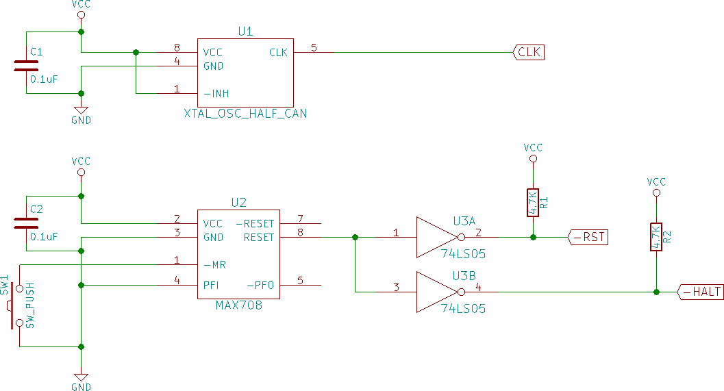
Note that a 74LS05 open-collector inverter is used to generate -RST and -HALT signals. The MAX708 has an active high reset output, which when fed through the ‘LS05 produces the active-low reset expected by the MC68008 (and pretty much every other device, too.)
I tested this portion of the circuit by using my multimeter to observe the -RST signal drop to about .3V when the reset button is pressed.
Glue logic
Pretty much any circuit with a CPU will need glue logic to let the peripheral devices know when they should transfer data over the data bus. The glue logic listens to control signals and addresses generated by the CPU, and generates chip enable signals for the various peripheral devices. The old school way of implementing glue logic is with discrete gates and decoders. The ever-so-slightly-newer school way to do this is with a programmable logic device (PLD). PLDs are nice because you just type in some equations describing the logic functions you want, assemble them, burn it onto your device, and you’re done. I’m using a GAL22V10, which I can program using my trusty Wellon VP-190 device programmer. Here’s the glue logic in the schematic (click for full size):

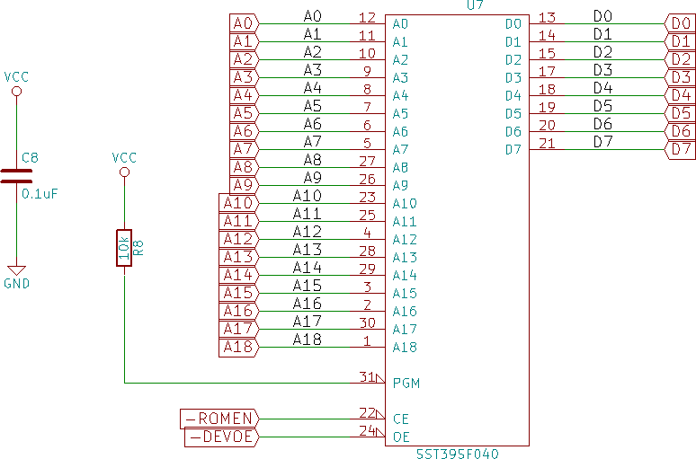
For this very preliminary version of my circuit, there are only two peripherals: an SST39SF040 flash ROM, and a 74LS374 8 bit output port. The memory map is very simple: the flash ROM is mapped in the low 512K of the address space, and the ‘374 is mapped in the high 512K of the address space.
Here are the GAL equations I used to generate the chip enable signals for the ROM and the output port:
/NROMEN = /NAS*RW*/A19
/NOPORTEN = /NAS*/NDS*/RW*A19
Note that /NAS, /NDS, and /RW are control signals from the CPU, and A19 is the high bit of the address bus. NAS is the address strobe, NDS is the data strobe, and RW is high for read cycles and low for write cycles. (I use the convention of prefixing active-low signals with ‘N’.)
There is also one additional signal generated by the glue logic:
NDEVOE = /RW
This signal inverts the CPU’s RW signal, and thus is low for read cycles and high for write cycles. This is useful for feeding into the active-low output enable input of memory chips (such as the flash ROM, and eventually the static RAM.) I shamelessly stole this idea from Steve Chamberlin’s 68 Katy project.
The glue.pld file defines all of the pin assignments, logic equations, etc. for the glue logic. It can be assembled using galasm.
After I burned the logic in the PLD, I wanted to be sure that it implemented the equations as intended. So, I built a test circuit using an AVR microcontroller (an atmega328, to be specific; click for full size):
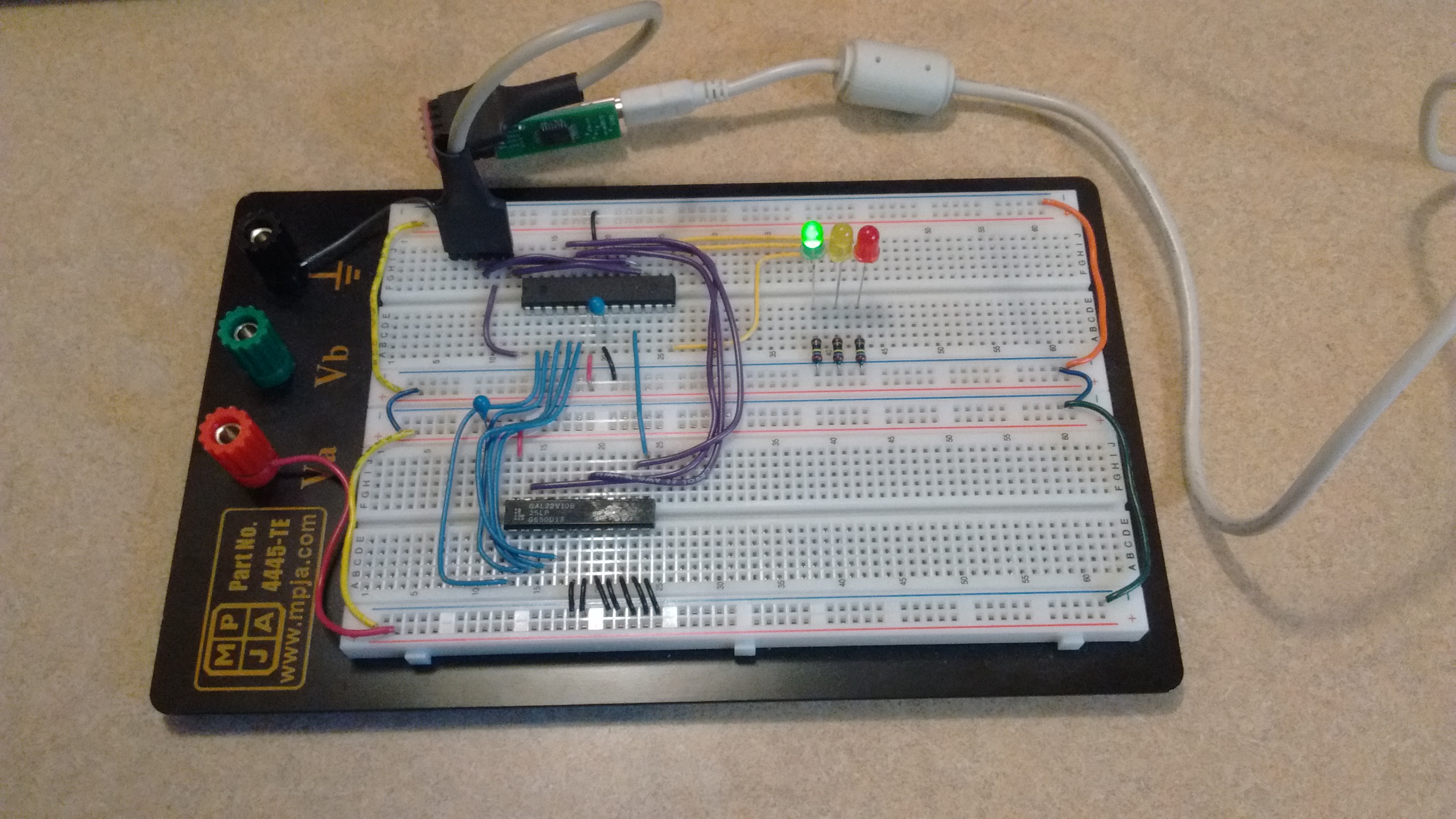
In the test circuit, the AVR pretends to be the CPU, generating control signals to feed to the PLD. Then, it reads the outputs of the PLD and checks that they are correct. The test circuit firmware program drives everything. As output, a green LED lights if all of the tests succeed, and red and yellow LEDs blink the test number and assertion number if an assertion failure occurs.
Once the test firmware was working correctly, the test circuit showed green, and I was reasonably confident that the PLD was working as intended.
Flash ROM, what to do about DTACK
My original plans involved using real, honest-to-goodness UV-eraseable EPROM for the firmware. This is all well and good from the standpoint of being authentically retro. The thing about EPROMs, however, is that they are mostly quite slow devices. I have some 120ns AMD 27C512 parts, which are pretty fast for EPROMs. These probably would work fine. But, in keeping with my goal of reducing complexity to an absolute minimum, I decided to go with a modern flash ROM, the SST39SF040-70, which is a 70ns part. Here’s why this is important.
The Motorola 68K series (of which the MC68008 is the most junior member) has an asynchronous bus cycle, where peripheral devices (or glue logic) must explicitly acknowledge the completion of a data transfer with the “DTACK” signal. This is kind of good, in that it allows you to interface with devices of varying speeds. The CPU will add wait states to read and write cycles to allow slow devices time to read or write data, the DTACK signal serving as an indication that the read or write has taken place. The downside is that this complicates the glue logic, because the timing of DTACK depends on which devices is being accessed, and some stateful logic is required to generate a delay of an appropriate length. I did not want to deal with this complexity up front.
The good news is that if only fast devices are used, such that no wait states are required, you can just tie the CPU’s DTACK input to ground. (There is a famous M68K technical newsletter called DTACK grounded named in honor of this idea.) So that’s what I did.
Eventually if I do decide to interface with any devices requiring wait states, I’ll implement some more sophisticated mechanism to generate DTACK, but only if necesssary.
So, with the DTACK issue sorted, interfacing with the flash ROM was fairly straightforward (click for full size):
An output port
An output port is a way for a microcomputer circuit to talk to the outside world (i.e., devices that aren’t directly wired into the circuit.) The idea is that a write to a particular memory location produces a pattern of high and low voltages depending on the bit pattern in the value written.
There are various 74-series devices that can be used to implement an output port. I used a 74LS374. The idea is that the data inputs of the ‘374 are connected to the data bus, and when a positive edge occurs on the Cp input, the values on the data bus are committed to D-type flip flops, whose outputs appear on the output pins. Wiring this into the circuit is straightforward (click for full size):
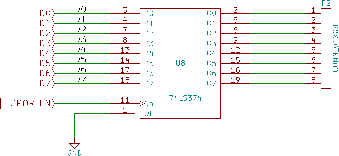
The outputs of LS family devices can sink 20 mA of current, which is enough to drive an LED. So, you can connect the cathode of an LED to one of the outputs, connect the anode to VCC through a resistor, and the LED will light up when a 0 (low voltage) is written to the corresponding data bit. In other words…blinkenlights.
Code!
Enough with the hardware already, let’s get some code on this thing!
GNU binutils and gcc are reasonably easy to build to target m68k, although you need to use fairly old versions. I wrote a script to build binutils/gcc on Linux, and adapted the rockboxdev.sh script to work on Cygwin (32 bit only). I think these scripts work: at the very least, you can read them to see what commands are needed to get a toolchain set up.
I could have tried to write a C program as my initial firmware, but in keeping with the philosophy of using the simplest possible approach, I wrote a tiny assembly language program, which I present to you in all its m68k glory:
One thing to note is the funny stuff at the beginning. On power-up, the M68K family CPUs load two 32-bit values from addresses 4 and 8. The first value becomes the value of the supervisor stack pointer (SSP), and the second value becomes the initial program counter (PC) value. Our code starts at address 8, hence the big-endian representation of 8 at address 4.
The code is pretty simple: an infinite loop that repeatedly writes the low 8 bits of %d0 to the output port, executes a delay loop, and toggles the low 8 bits in %d0. The initial bit pattern 0x55 has alternating 0 and 1 bit values, and inverting these bits will cause each individual LED to toggle on each iteration of the main loop.
I used my Wellon VP-190 to program this firmware image onto the flash ROM. (Digression: I actually bought a laptop just so I could install Windows to use the Wellon software. Happily, I found a nice used Thinkpad T61 on Ebay for only $36 shipped.)
Building it! and mysterious behavior
I tried to be methodical in building and testing each component, although at some point you just have to wire it up and hope for the best.
I started by adding the glue logic PLD to the circuit, connecting it to power and feeding it the appropriate CPU control and address signals, and seeing if the circuit still worked in free run mode (with all of the data lines tied to ground.) It did. (I verified the free run by connecting LEDs through a 74LS04 inverter driven from the high 4 address lines, and observing that they toggled appropriately as the CPU attempted to load instructions sequentially through its address space.)
Next, I wired up the flash ROM. This was a bit fiddly because there are 18 address lines and 8 data lines to be connected, as well as two control signals (-ROMEN and -DEVOE) from the glue logic, so quite a few wires. After connecting all of these, I applied power, and again tested the circuit in free run mode (data lines tied to ground.) Things still looked good.
Now for the moment of truth: I connected the CPU’s data lines to the flash ROM’s data lines and powered the circuit on. I’m not sure exactly what I was expecting to happen, since the output port and its LEDs were not yet present. I was expecting that the LEDs monitoring the high address lines (A16..A19) would be useful, since the firmware lies entirely in low ROM (it’s only 46 bytes and it’s loaded at address 0.) I did expect that the A19 LED would be on some of the time since the output port is accessed at address 0x80000. What I actually saw was the A16..A19 LEDs lighting at low intensity, which is consistent with rapid toggling. A19 I expected, but the others…WTH?
Time to cheat
I work in a department where almost all of my colleagues are engineers. So, I asked my colleague James to help me use a logic analyzer to figure out what was going on. We weren’t terribly systematic about our approach: I just tapped most of the CPU control signals (-AS, RW, etc.), the low address lines, the -ROMEN and -DEVOE signals from the glue logic, and (most significantly) the data lines. Here’s the whole mess (click for full size):
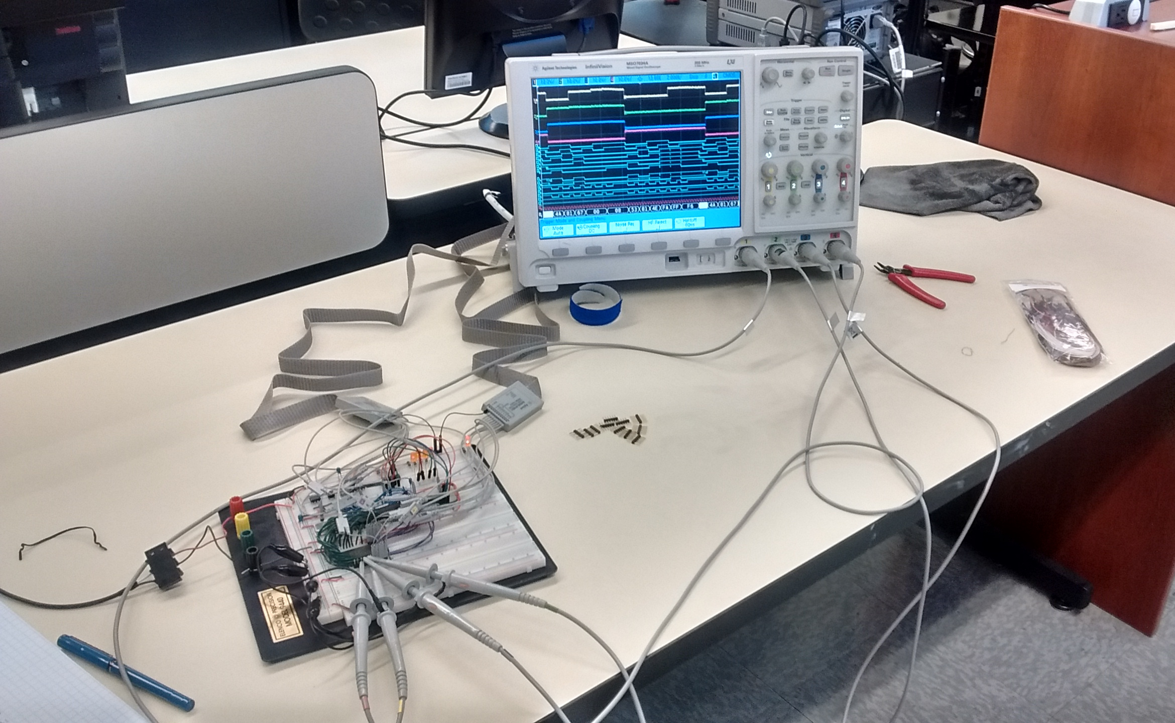
What became apparent fairly quickly was that the values on the data bus were, indeed, the opcodes of my firmware program! We were even able to see repetitions of the instructions in the delay loop. This was a pretty good indication that the code in the flash ROM was being executed.
I’m still not sure why the LEDs on A16..A18 were toggling, but I’m hoping to figure that out sometime soon.
Output port, and triumph
Long story short, I wired up the output port, connected the LEDs, and…
Success!
Just for fun, here’s a picture of the whole thing in its current form (click for full size):
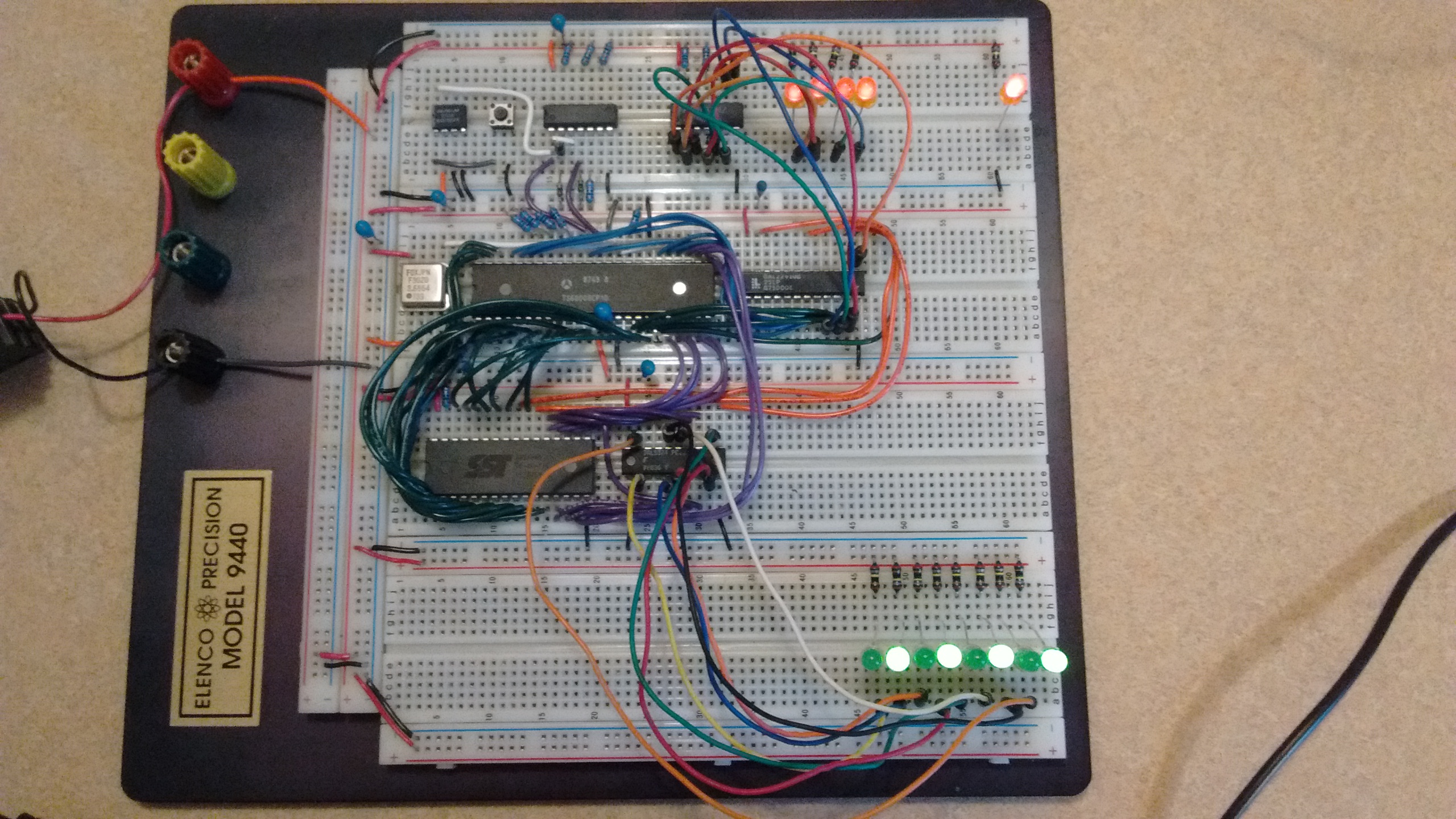
White wires are the reset and clock signals, light blue wires are control signals from the CPU, orange wires are outputs from the glue logic, green wires are the address bus, purple wires are the data bus.
Conclusions, what next
I realize that this was more than a month of work to achieve a result that you could accomplish with an AVR microcontroller in about 10 minutes. In a way, that’s what makes it so cool!
My next step is to add a static RAM chip. There are some technical reasons why its useful to map RAM in the low part of the address space, so I also plan to update the glue logic to dynamically remap the ROM into the high part of the address space. I also plan to move the output port, and perhaps get closer to a “permanent” memory map for the system.
Stay tuned…
blog comments powered by Disqus