In the previous installment, I described the clock and reset circuit I’m using for my MC68008 computer project.
In this post, I describe getting the CPU to execute instructions for the first time. Not interesting instructions, but instructions nonetheless. This is an important milestone; at the very least, it shows that it is possible that the TS68008CP10 chip I’m using is working. (I’ll reserve final judgement until it executes some instructions that I write.)
What is a free run?
A free run is a circuit in which a CPU executes meaningless instructions. In the case of the MC68008, the (single-byte) opcode 0 is the nop instruction, which does nothing except incrementing the program counter by 1. If we tie all of the data bus lines to ground, the CPU will read all 0 bits each time it fetches an instruction, and thus the CPU will do nothing but execute nop instructions. This sounds boring, except that by observing the highest address line (A19), we can watch the CPU cycle through the address space. The A19 line will change state every 524,288 instructions, as the program counter moves from the low 512K of the address space to the high 512K.
Free run circuit
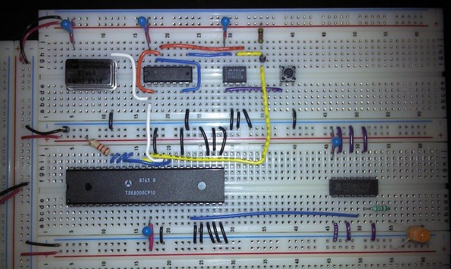
I adapted the free run circuit from a nice project handout from a course at Texas A&M University. I used my own clock and reset circuit, but otherwise I followed the circuit described in the handout. The idea is to tie various lines that control the CPU, such as -DTACK, -BR, and -BERR to either ground or VCC as appropriate. For example, by tying -DTACK to ground we force each bus cycle to end immediately, effectively running the CPU without any wait states.
Rather than generating separate -RESET and -HALT signals from the reset circuit, I feed a single -RST signal into both the -RESET and -HALT pins on the CPU. I’ve read that this is acceptable. There are some situations in which it is advantageous to separate -RESET and -HALT (such as single-step execution), but in the interest of simplicity I’m not worrying about those cases.
I followed the recommendation in the handout to feed the A19 signal to a gate in a 74HCT04 inverter. (The handout actually suggested a 74LS04, but I prefer CMOS parts.) The output of the gate is then used to turn an LED on and off.
Here’s a picture of the circuit on the breadboard:
It blinks! But not (seemingly) at the correct rate
Well, long story short, I wired it up and it seems to work. The LED blinks!
Is it working correctly? The TS68008 datasheet seems to indicate (in Table 7.15) that a nop instruction requires 8 cycles to execute. With an 8 MHz system clock, that’s an even 1,000,000 instructions per second. There are 1,048,576 nop instructions in the address space, meaning that it should take just a bit over 1 second for the CPU to cycle through the entire address space.
However…in the actual circuit, the LED seems to be blinking twice per second. Could it be that a nop actually needs only 4 cycles to execute? That seems unlikely, since a bus cycle alone requires a minimum of 4 cycles.
Perhaps I’m not understanding something. The -RESET signal is remaining high (i.e., not asserted), so it doesn’t appear that either the MAX1232 or the CPU is generating spurious reset pulses. As far as I can tell, the duty cycle of the LED seems to be exactly 50%, which would be the case if the CPU really is cycling through its address space.
What next?
I would like to figure out what is going on. Probably I will ask my colleague Greg Link to help me use a logic analyzer to see if the other address lines are toggling in the expected pattern. (Working at an engineering school is sweet.) If they are, then I suppose that it really is working correctly. I may also try a different TS68008 chip (I have 4 of them), and possibly a slower oscillator module (although I don’t have any on hand.)
Assuming I am satisfied that the free run is working, then the next step will be to connect an EPROM and execute some actual code.
blog comments powered by Disqus