Unlike modern CPUs and microcontrollers, the MC68008 requires an external clock signal. It also requires an external reset signal in order to initialize properly.
System clock
For the system clock, I am using a crystal oscillator module. These are really easy to use: you just supply power and it generates a square wave of a specified frequency. The MC68008 requires a minumum clock frequency of 2 MHz. I’m using an 8 MHz oscillator, which means a clock cycle occurs every 125 ns. My TS68008 is rated for 10 MHz, so I could use a 10 MHz clock if I wanted to.
In theory I could have built a clock circuit, but my design philosophy is that I don’t build anything for which a ready-made solution is available.
Reset pulse
To initialize when powered up, the MC68008’s -RESET and -HALT pins must be driven low for 100 ms. This reset pulse could be generated using a 555 timer; however, a nice off the shelf solution exists in the Maxim MAX1232.
The MAX1232 is a small (8 pin) IC which performs two functions:
- Generating a reset pulse on system power-up, or when a reset button is pressed
- Generating a reset pulse when a system failure is detected
The second function makes the MAX1232 a “watchdog”; if an input pin (-ST) is not toggled with a specified minimum frequency, a reset pulse is generated. The idea is that the system’s microprocessor will use an I/O pin to toggle the -ST pin periodically. In the event of a failure such as a software crash or lock up, the MAX1232 will notice the failure to toggle -ST and reset the system.
I don’t really need the watchdog function at this point, so I will use a clock signal derived from the main system clock to toggle this pin.
The MAX1232 is readily available. You can request samples from Maxim’s website. You can also buy them from pretty much any electronics component distributor. Ebay is also an option, although I wonder about the authenticity of parts sold on Ebay.
RAM/ROM mapping at startup
When the MC68008 initializes, it starts fetching instructions at memory address 0. For this reason, it is necessary to have some form of ROM (such as an EPROM) mapped at address 0, so that the firmware can take control.
In theory we could just leave ROM mapped at address 0 permanently. Unfortunately, the CPU’s interrupt vector table is located at address 0. If we want to allow interrupts to be handled in a reasonable way as the system runs, we need to have RAM mapped at address 0. So, we need a way to have ROM mapped at address 0 on startup, but RAM mapped during normal operation.
My solution is to use a 74HCT393 counter chip. This chip is two 4-bit counters which increment on a low-to-high clock transition. If we cascade the two 4-bit counters, we get an 8-bit counter. The counter is reset (cleared) by the reset signal generated by the MAX1232, and when the reset pulse ends the counter is incremented by low-to-high clock transitions. The most significant bit of the 8-bit counter effectively divides the system clock by 256. This signal will be low for the first 128 clock cycles following reset, high for the next 128 clock cycles, etc.
The system’s glue logic can use this signal to map the firmware EPROM at address 0 during the first 128 cycles, and then map the static RAM at address 0 subsequently. This gives the firmware a chance to jump from a low code address to a permanent code address. (I plan to map the EPROM in the high 64K of the address space.) On the schematic, I am calling this signal CLKDIV256.
As an additional use for this signal, I am feeding it to the -ST pin of the MAX1232. This ensures that a watchdog reset will not occur (as mentioned above).
-RST and -HALT
The MC68008 has -RESET and -HALT pins which, if driven low, cause the CPU to reset. These pins are bidirectional, meaning that they are inputs and outputs simultaneously. The idea is that all devices in the system should reset themselves if the system-wide -RST signal is asserted. The reset circuit (in our case, the MAX1232) can force a reset, but via software the CPU can also force a reset of external devices by driving the -RST signal low.
To allow this signal to be bidirectional, all devices connected to it must use open collector output. An open collector output is normally held high using a pull-up resistor. Any connected device may force the line low by sinking current, pulling the voltage down to a low logic level. Open collector outputs are sometimes called “wired-or” because (for an active-low signal such as -RESET) any device outputting a low level causes any devices reading the signal to see a logic low.
Happily, the MAX1232 has an -RST pin that is an open collector output. This pin can be connected directly to the -RESET and -HALT pins of the MC68008 to perform the initial reset. This signal will also connected to the reset inputs of peripheral devices as needed.
That’s it, really
The final circuit is pretty simple:
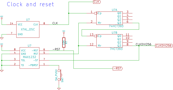
Note that I haven’t annotated the schematic with final component names yet. Nor are decoupling capacitors included.
A photo of the circuit on the breadboard:
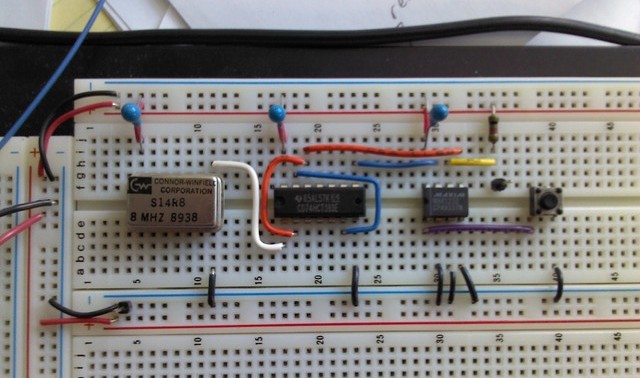
The header pin in column 35 is a test point for the reset signal. My multimeter showed the voltage dropping from VCC to about .3V when the reset button is pressed.
What’s next?
Next I will add the MC68008 in free run mode. The idea is to tie the data bus lines to ground: the CPU will then read 0 on every memory reference. Since 0 corresponds to the nop instruction, which does nothing, the CPU will continuously fetch nop instructions, cycling though the entire address space over and over.
Free run clearly doesn’t accomplish anything useful. However, we can observe the CPU’s high address line (A19) toggling on and off, and gain confidence that the CPU is operational.
blog comments powered by Disqus